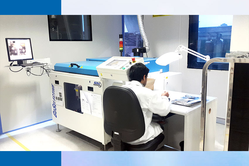
Customised Solutions

Customised Solutions

ADTL offers a comprehensive range of specialized services that enhance product performance, reliability, and manufacturability. Our advanced capabilities ensure that every assembly meets the highest quality and durability standards required for mission-critical applications.

Selective Soldering

  • Accurate soldering for lead-free components.
  • Preheating, solder bath control, flux verification, inspection for solder splashes/alignment, cleaning within 8 hours.
  • Nitrogen-controlled & compliant with IPC standards.

Conformal Coating

  • Protect PCBAs from moisture, dust, chemicals, and environmental stress.
  • Coating Types: Acrylic, Polyurethane; Thickness: 25–250 µm.
  • Standards: IPC-610, IPC-CC-830, IPC-TM-650; RoHS compliance.
  • Controls: Masking, spray process, UV inspection, adhesion & boiling tests, strict ESD compliance.

Flying Probe Testing (FPT)

  • Fixture-less electrical verification of PCBAs.
  • Dual-sided flying probe tester, 4 flying probes, 2 Open fix probes, high-resolution cameras.

Measurement Ranges:

  • Resistors: 0 Ω–40 MΩ
  • Capacitors: 4 pF–40 mF
  • Inductors: 4 µH–400 H
  • Diodes/Transistors: 0.1–2.5 V
  • Shorts/Opens: 1 Ω–400 Ω

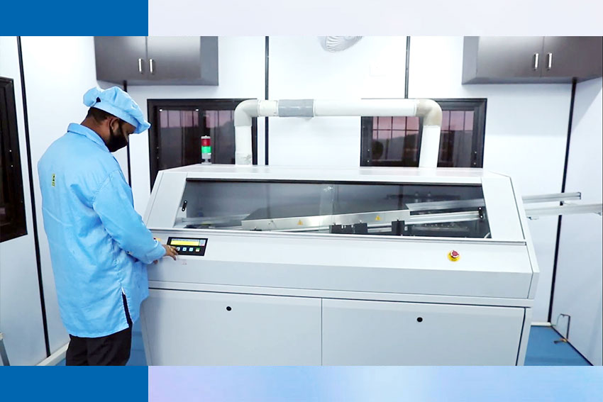
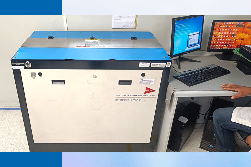
Prototyping, small/medium production, traceability via barcode/2D code.

Wave Soldering

  • Our automated wave soldering process supports through-hole components with strong, consistent solder joints suitable for high-volume production.
  • PCB width of 400–450 mm; Leaded & lead-free solder; IPC-A-610 Class 2 & 3.
  • Conveyor width adjustment, pre-inspection, flux/solder maintenance, post-inspection, ESD/MSD compliance, PPE usage, FOD prevention.

Pressfit Technology

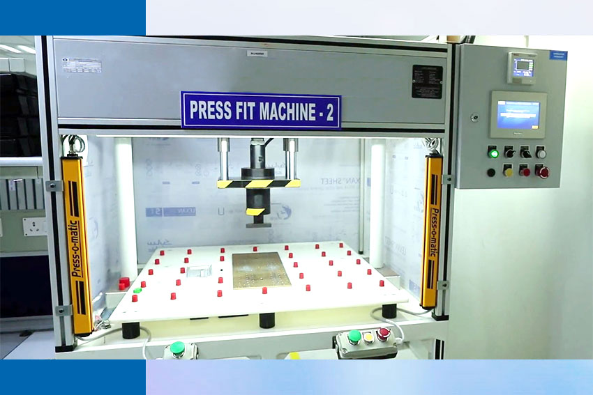
Mechanical & electrical connector assembly without solder.

Specs:

  • Max rotary speed: 3000 rpm; Torque: 4.6 N-m
  • Load cell: 5 TON; Max load: 3000 kg
  • Servo travel: 200 mm; Travel error: 170 mm

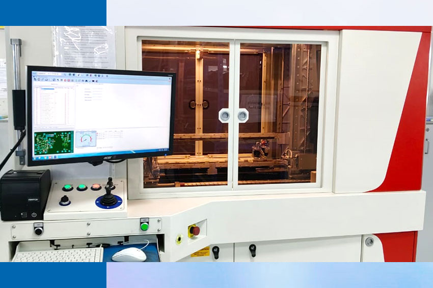
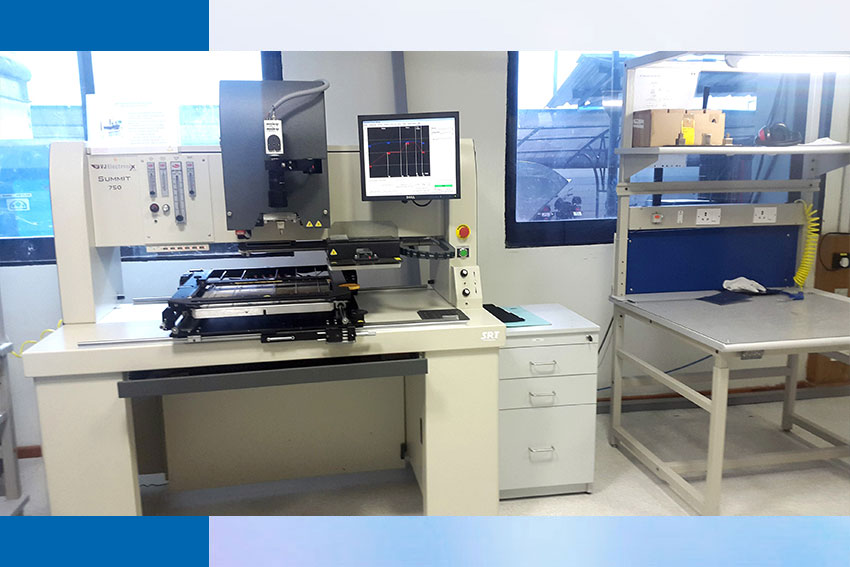
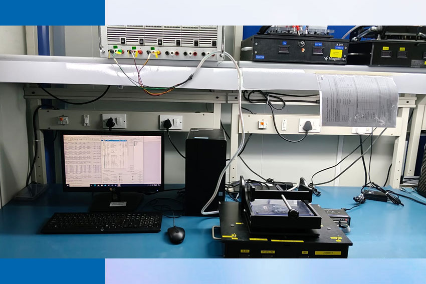
Optical inspection per IPC-9797.

Environmental Screening & Vibration Testing

  • Environmental: Temp cycling –55°C to +125°C, high humidity up to 95% RH, burn-in & operational testing.
  • Vibration: Frequency 5 Hz–3 kHz, acceleration 20–30 g, modes: Sine/Random/Sine-on-Random.
  • Standards: MIL-STD-810, IEC 60068, DO-160.

Highly Accelerated Stress Screening (HASS)

  • Identify early-life failures.
  • Specs: Temp cycling up to 60°C/min, vibration 5–25 g RMS, custom stress profiles.
  • Applications: Defense, aerospace, high-reliability electronics.

BGA / Component Rework & Reballing

  • Reballing of BGA pitch ≥0.3 mm, leaded & lead-free solder, IPC-7095 compliant, X-ray verification.
  • Rework as per IPC-7711/7721, profile-controlled reflow, traceability maintained.
  • Repair: Component replacement, trace repair, micro-stencil printing, functional testing, customer approval for critical products, full documentation.

Ionic Contamination Test

  • 75% IPA + 25% DI water; verified with hydrometer.
  • Process: Ionograph calibration, verification, PCBA testing for resistivity/conductivity.
  • Output: Cleanliness report against acceptance criteria.

Boundary Scan Testing (BST)

  • Tests PCB interconnections without physical probing using IEEE 1149.1.
  • Detect opens, shorts, faulty solder joints in complex PCBs.
  • Advantages: High test coverage for dense/multilayer boards, reduces manual probing.
  • Applications: Production testing, IC in-system programming, debugging complex boards before final assembly.

Design for Manufacturing (DFM)

At ADTL, we ensure that every product is optimized for smooth and reliable manufacturing. After receiving the customer’s kit, our engineering team conducts a thorough DFM review to identify any design or assembly issues that may affect quality, yield or production efficiency.

If we find any concerns, we share a detailed DFM report with the customer. This helps customers correct the issues in future batches, reduce rework, improve consistency and achieve better long-term manufacturability.

Our proactive DFM support ensures faster production, fewer defects, and overall cost savings for our customers

Replating / Degolding

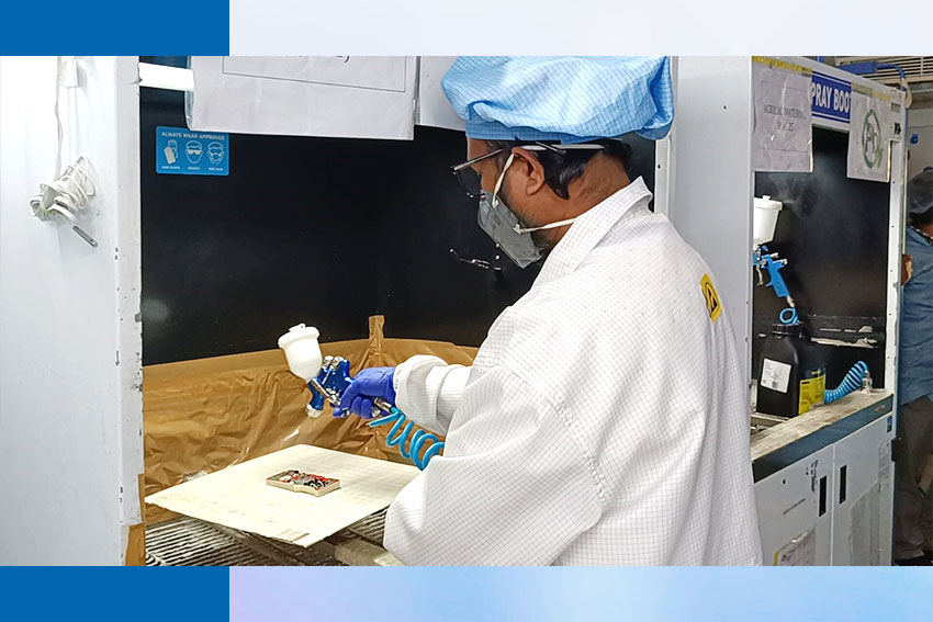
We provide precise reballing, replating and degolding services to ensure proper solderability and improved reliability of components, especially for reworked or legacy parts.

Key Specs:

  • Double tinning ~95% coverage (SMT, PTH, other terminals) per J-STD-001.
  • Maximum PCB size: 500 × 500 mm; component height: Top 65 mm, Bottom 30 mm.
  • Solder bath: 450°C; Preheater top: 250°C, bottom: 200°C.
  • Program verification, QA batch clearance, ESD/MSD compliance, FOD prevention, traceability.